logo
Ürünler
Ev / Ürünler / JEDEC IC Tepsileri /

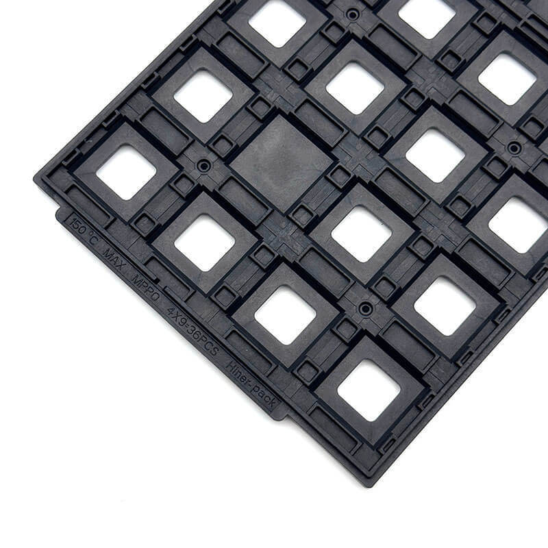
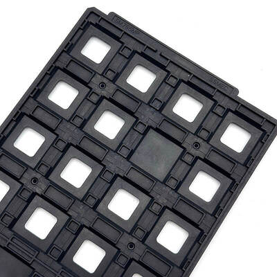
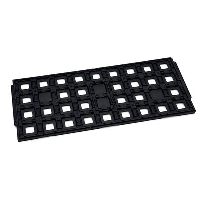
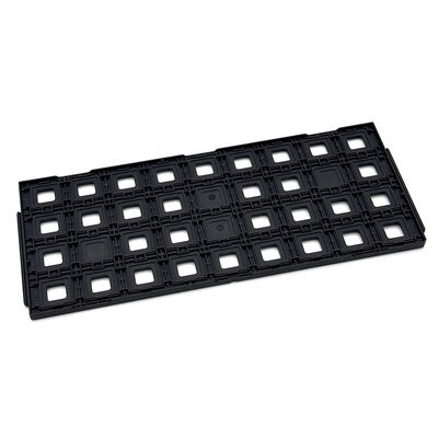
Durable JEDEC IC Trays for Dust-Free Semiconductor Packaging

Durable JEDEC IC Trays for Dust-Free Semiconductor Packaging

Marka Adı: Hiner-pack
Model Numarası: HN25006
Moq: 500 adet
fiyat: $1.35~$2.38(Prices Are Determined According To Different Incoterms And Quantities)
Ödeme Şartları: T/T
Tedarik Yeteneği: 2000 adet/gün
Ayrıntılı Bilgiler
Menşe yeri:
Çin
Sertifika:
ROHS, ISO
Tepsi Ağırlığı:
Genellikle Kavite Başına 500 Grama Kadar Değişir
Renk:
Siyah
Kalite Güvencesi:
Teslimat garantisi, güvenilir kalite
Kavite Boyutu:
322,6x135,9x7,62 mm
Incoterms:
EXW, FOB, CIF, DDU, DDP
Kalıp Tipi:
Enjeksiyon
Yeniden kullanılabilir:
Evet
Tepsi Şekli:
Dikdörtgen
Temiz Sınıf:
Genel ve Ultrasonik Temizleme
IC Türü:
BGA,QFP,QFN,LGA,PGA
Paketleme seviyesi:
Taşıma Paketi
Düzlük:
0,76 mm'den az
Kapasite:
4x9=36 Adet
Ambalaj bilgileri:
karton, palet
Yetenek temini:
2000 adet/gün
Ürün Tanımı
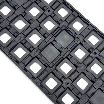
Durable JEDEC IC Trays for Dust-Free Semiconductor Packaging
Shield delicate semiconductor components from dust and damage during packaging operations. Minimize contamination risks effectively. Built with durable structure to meet JEDEC standards for reliable industrial use. Seeking trusted tray solutions for secure semiconductor packaging?

Fit automated packaging lines and cleanroom environments perfectly. Perform steadily in component handling and packaging procedures. Adapt to diverse semiconductor packaging processes smoothly.

Enable safe component storage and logistics. Support custom designs to meet specific packaging demands. Deliver tailored solutions for unique semiconductor manufacturing requirements.
Key Features/ Benefits 
  • Deliver durable construction.
  • Reduce dust contamination.
  • Dust minimization.
  • Component protection.
  • Flexible customization.
Specifications
Brand Hiner-pack
Model HN25006
Material  MPPO
Package Type JEDEC
Color Black
Resistance 1.0×10⁴ - 1.0×10¹¹ Ω
Outline Line Size 322.6x135.9x7.62 mm
Cavity Size 16×9.5×4.72 mm
Matrix QTY 4x9=36 PCS
Warpage MAX 0.76mm
Service Accept OEM, ODM
Custom Pocket Options Available
Applications
Apply to semiconductor wafer level packaging, IC performance testing, die sorting, wafer fabrication, and device assembly. Adapt to cleanroom manufacturing, automated production lines, precision component handling, and high-temperature processing workflows. Ensure stable performance in strict dust-free environments.

Support component long-term storage, inter-factory logistics, production turnover, vacuum packaging, and sample shipment operations. Meet diverse requirements for semiconductor packaging, quality inspection, supply chain management, and electronic component distribution.
Packaging & Shipping/ Services
Offer targeted customization for JEDEC IC trays tailored to packaging and transportation needs. Collaborate closely with teams to design cavity shapes, anti-slip structures, and shock-absorbent materials for secure component handling during packaging and long-distance logistics. Develop anti-static or dust-sealed variants, and validate prototypes through vibration and drop tests. Deliver personalized tray solutions that safeguard semiconductor components throughout packaging, loading, and inter-factory or global shipment processes.
About Us:
Hiner-pack® was founded in 2013. It is a high-tech enterprise that integrates Design, R&D, Manufacturing, Sales of IC packaging and testing, as well as semiconductive wafer fabrication process in automated handling, carrying, and transportation to provide customers with turnkey services.

Why Choose Us:

  • Rich experience in JEDEC / IC / waffle pack trays
  • In-house mold design capability
  • Fast prototype development
  • Strict QC process
  • Stable supply for global semiconductor customers